1. SVD (System View Description)
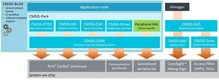
1.1. CMSIS (Cortex Microcontroller Software Interface Standard)
- ARM에서 제정하는 Cortex-M 시리즈의 소프트웨어 인터페이스 표준 (최신 버전에서는 Cortex-A 시리즈도 고려되는 듯)
- Cortex-M 코어를 사용하는 다수의 MCU 제조사들의 호환성 확보를 위해 ARM <-> 각 제조사간 협력을 통해 제정
https://www.keil.com/pack/doc/CMSIS/General/html/index.html
1.2. CMSIS-SVD
- MCU의 peripheral, register 정보 등을 xml 파일 형태로 기술
(1) SVD Description Format

https://arm-software.github.io/CMSIS_5/SVD/html/svd_Format_pg.html
(2) SVD File Example
- https://github.com/cmsis-svd/cmsis-svd-data
펼치기
<?xml version="1.0" encoding="utf-8"?>
<device schemaVersion="1.1" xmlns:xs="http://www.w3.org/2001/XMLSchema-instance" xs:noNamespaceSchemaLocation="CMSIS-SVD.xsd" >
  <vendor>ARM Ltd.</vendor>                                       <!-- device vendor name -->
  <vendorID>ARM</vendorID>                                        <!-- device vendor short name -->
  <name>ARM_Example</name>                                        <!-- name of part-->
  <series>ARMCM3</series>                                         <!-- device series the device belongs to -->
  <version>1.2</version>                                          <!-- version of this description, adding CMSIS-SVD 1.1 tags -->
  <description>ARM 32-bit Cortex-M3 Microcontroller based device, CPU clock up to 80MHz, etc. </description>
  .............................
  <cpu>                                                           <!-- details about the cpu embedded in the device -->
    <name>CM3</name>
    <revision>r1p0</revision>
    <endian>little</endian>
    <mpuPresent>true</mpuPresent>
    <fpuPresent>false</fpuPresent>
    <nvicPrioBits>3</nvicPrioBits>
    <vendorSystickConfig>false</vendorSystickConfig>
  </cpu>
  <addressUnitBits>8</addressUnitBits>                            <!-- byte addressable memory -->
  <width>32</width>                                               <!-- bus width is 32 bits -->
  <size>32</size>                                                 <!-- this is the default size (number of bits) of all peripherals
                                                                       and register that do not define "size" themselves -->
  <access>read-write</access>                                     <!-- default access permission for all subsequent registers -->
  <resetValue>0x00000000</resetValue>                             <!-- by default all bits of the registers are initialized to 0 on reset -->
  <resetMask>0xFFFFFFFF</resetMask>                               <!-- by default all 32Bits of the registers are used -->

  <peripherals>
    <!-- Timer 0 -->
    <peripheral>
      <name>TIMER0</name>
      <version>1.0</version>
      <description>32 Timer / Counter, counting up or down from different sources</description>
      <groupName>TIMER</groupName>
      <baseAddress>0x40010000</baseAddress>
      <size>32</size>
      <access>read-write</access>

      <addressBlock>
        <offset>0</offset>
        <size>0x100</size>
        <usage>registers</usage>
      </addressBlock>

      <interrupt>
        <name>TIMER0</name>
        <description>Timer 0 interrupt</description>
        <value>0</value>
      </interrupt>

      <registers>
      <!-- CR: Control Register -->
        <register>
          <name>CR</name>
          <description>Control Register</description>
          <addressOffset>0x00</addressOffset>
          <size>32</size>
          <access>read-write</access>
          <resetValue>0x00000000</resetValue>
          <resetMask>0x1337F7F</resetMask>

          <fields>
            <!-- EN: Enable -->
            <field>
              <name>EN</name>
              <description>Enable</description>
              <bitRange>[0:0]</bitRange>
              <access>read-write</access>
              <enumeratedValues>
                <enumeratedValue>
                  <name>Disable</name>
                  <description>Timer is disabled and does not operate</description>
                  <value>0</value>
                </enumeratedValue>
                <enumeratedValue>
                  <name>Enable</name>
                  <description>Timer is enabled and can operate</description>
                  <value>1</value>
                </enumeratedValue>
              </enumeratedValues>
            </field>
            ..........................................
          </fields>
        </register>
        <!-- SR: Status Register -->
        <register>
          <name>SR</name>
          <description>Status Register</description>
          <addressOffset>0x04</addressOffset>
          <size>16</size>
          <access>read-write</access>
          <resetValue>0x00000000</resetValue>
          <resetMask>0xD701</resetMask>

          <fields>
            <!-- RUN: Shows if Timer is running -->
            <field>
              <name>RUN</name>
              <description>Shows if Timer is running or not</description>
              <bitRange>[0:0]</bitRange>
              <access>read-only</access>
              <enumeratedValues>
                <enumeratedValue>
                  <name>Stopped</name>
                  <description>Timer is not running</description>
                  <value>0</value>
                </enumeratedValue>
                <enumeratedValue>
                  <name>Running</name>
                  <description>Timer is running</description>
                  <value>1</value>
                </enumeratedValue>
              </enumeratedValues>
            </field>
            .............................
          </fields>
        </register>
        .............................
    </peripheral>

    <!-- Timer 1 -->
    <peripheral derivedFrom="TIMER0">
      <name>TIMER1</name>
      <baseAddress>0x40010100</baseAddress>
      <interrupt>
        <name>TIMER1</name>
        <description>Timer 1 interrupt</description>
        <value>4</value>
      </interrupt>
    </peripheral>
    .......................
  </peripherals>
</device>
2. SVD Files
- Cortex-M 시리즈를 사용하는 MCU의 svd 파일들이 벤더별로 수집되어있음
- 필요한 Vendor - MCU의 svd를 다운로드
.
├── Allwinner-Community
│   ├── D1-H.svd
│   └── README.md
├── ARM_SAMPLE
│   ├── ARM_Sample.svd
│   └── CMSDK_CM3.svd
├── ArteryTek
│   ├── AT32A403Axx_v2.svd
│   ├── AT32F402xx_v2.svd
│   ├── AT32F403Axx_v2.svd
│   ├── AT32F403xx_v2.svd
..........................
└── STMicro
    ├── Contents.txt
    ├── fill_contents.py
    ├── License.html
    ├── STM32F030.svd
    ├── STM32F031x.svd
    ....................
    ├── STM32F100xx.svd
    ├── STM32F101xx.svd
    └── STM32W108.svd
3. leveldown-security/SVD-Loader-Ghidra
- SVD 파일을 ghidra에 로드하여 레지스터 정보를 확인 가능
3.1. Setup
(1) Clone git repository
git clone https://github.com/leveldown-security/SVD-Loader-Ghidra.git(2) Load SVD-Loader.py to Ghidra
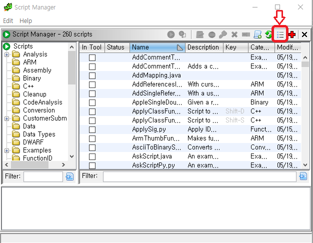
1) Menu > Window > Script Manager
2) Append bundle directory
3) Run 'SVD-Loader.py'
4) Select SVD file
설치화면


3.2. Result
- 정상적으로 svd 파일을 로드할 경우 아래와 같이 레지스터 정보 확인 가능


4. Using SVD file in GDB for Cortex-m debugging
- SVD 파일을 gdb에 로드하여 디버깅 과정에서 레지스터 상태 확인 가능
4.1. Setup
(1) Clone & Run setup.py
git clone https://github.com/bnahill/PyCortexMDebug.git
cd PyCortexMDebug
python setup.py install --user
(2) Configure .gdbinit
cat << EOF >> ~/.gdbinit
# https://yairgadelov.me/using-svd-file-in-gdb-for-cortex-m-debugging/
# Setup GDB to interpret in Python
pi
import os,subprocess,sys
# Execute a Python using the user's shell and pull out the sys.path (for site-packages)
paths = subprocess.check_output('python -c "import os,sys;print(os.linesep.join(sys.path).strip())"',shell=True).decode("utf-8").split()
# Extend GDB's Python's search path
sys.path.extend(paths)

# load svd tools
from cmdebug.svd_gdb import LoadSVD
from cmdebug.dwt_gdb import DWT
DWT()
LoadSVD()
EOF
4.2. Usage
(1) Load
peda-arm > svd_load ~/gits/der_bug_hunter/SMAInverter/analysis_stp_2.83/gdb/STM32F103.svd
Loading SVD file ~/gits/der_bug_hunter/SMAInverter/analysis_stp_2.83/gdb/STM32F103.svd...
peda-arm >
peda-arm > svd
Available Peripherals:
FSMC: Flexible static memory controller
PWR: Power control
RCC: Reset and clock control
GPIOA: General purpose I/O
GPIOB: General purpose I/O
GPIOC: General purpose I/O
GPIOD: General purpose I/O
GPIOE: General purpose I/O
.............................................
NVIC: Nested Vectored Interrupt Controller
USB: Universal serial bus full-speed device interface
OTG_FS_DEVICE: USB on the go full speed
OTG_FS_GLOBAL: USB on the go full speed
OTG_FS_HOST: USB on the go full speed
OTG_FS_PWRCLK: USB on the go full speed
ETHERNET_MMC: Ethernet: MAC management counters
ETHERNET_MAC: Ethernet: media access control
ETHERNET_PTP: Ethernet: Precision time protocol
ETHERNET_DMA: Ethernet: DMA controller operation(2) Dump Register
peda-arm > svd GPIOA
Warning: GPIO could prefix match any of: GPIOA, GPIOB, GPIOC, GPIOD, GPIOE, GPIOF, GPIOG
Registers in GPIOA:
        CRL:       0x44444444  Port configuration register low (GPIOn_CRL)
        CRH:       0x88844444  Port configuration register high (GPIOn_CRL)
        IDR:       0x00000000  Port input data register (GPIOn_IDR)
        ODR:       0x0000A000  Port output data register (GPIOn_ODR)
        BSRR:  (not readable)  Port bit set/reset register (GPIOn_BSRR)
        BRR:   (not readable)  Port bit reset register (GPIOn_BRR)
        LCKR:      0x00000000  Port configuration lock register
peda-arm > svd GPIOA CRL
Fields in GPIOA > CRL:
MODE0: 0x0 Port n.0 mode bits
CNF0: 0x1 Port n.0 configuration bits
MODE1: 0x0 Port n.1 mode bits
CNF1: 0x1 Port n.1 configuration bits
MODE2: 0x0 Port n.2 mode bits
CNF2: 0x1 Port n.2 configuration bits
MODE3: 0x0 Port n.3 mode bits
CNF3: 0x1 Port n.3 configuration bits
MODE4: 0x0 Port n.4 mode bits
CNF4: 0x1 Port n.4 configuration bits
MODE5: 0x0 Port n.5 mode bits
CNF5: 0x1 Port n.5 configuration bits
MODE6: 0x0 Port n.6 mode bits
CNF6: 0x1 Port n.6 configuration bits
MODE7: 0x0 Port n.7 mode bits
CNF7: 0x1 Port n.7 configuration bits(3) Formatting
peda-arm > svd/b GPIOA
Registers in GPIOA:
        CRL:   0b01000100010001000100010001000100  Port configuration register low (GPIOn_CRL)
        CRH:   0b10001000100001000100010001000100  Port configuration register high (GPIOn_CRL)
        IDR:   0b00000000000000000000000000000000  Port input data register (GPIOn_IDR)
        ODR:   0b00000000000000001010000000000000  Port output data register (GPIOn_ODR)
        BSRR:                      (not readable)  Port bit set/reset register (GPIOn_BSRR)
        BRR:                       (not readable)  Port bit reset register (GPIOn_BRR)
        LCKR:  0b00000000000000000000000000000000  Port configuration lock register